Introduction
For decades, the dominant paradigm in chip design was the monolithic SoC (System-on-Chip) — integrating as many functional blocks as possible into a single die manufactured on a single process node. This approach maximized integration, minimized inter-chip communication latency, and simplified the system-level design. It worked brilliantly as long as transistor scaling continued to deliver regular improvements in density, performance, and cost per transistor.
In 2026, the industry has made a decisive shift to chiplet-based disaggregated architectures and advanced 3D packaging — driven by the economics of transistor scaling at advanced nodes and the physical limits of monolithic die size. AMD's EPYC processors, Intel's Ponte Vecchio GPU, TSMC's System-on-Integrated-Chips (SoIC), and virtually every new AI accelerator architecture use some form of chiplet disaggregation and advanced packaging. This is not a trend — it is the new default architecture for high-performance semiconductor design.
Where this is written from: I design robotics, UAV and industrial-automation systems and the software that runs them. I do not design chiplets or advanced packaging, and this is a reading of published material from AMD, Intel, TSMC and the UCIe consortium rather than a first-hand account of a packaging programme.
What draws me to it is structural rather than technical. Most of the interesting engineering problems I run into happen at the boundaries between layers — between mechanics and control, between embedded firmware and the network, between a machine and the software watching it. Chiplets are that same story playing out one level down: an integration boundary that used to sit on a circuit board has moved inside a package. Boundaries that move tend to take their failure modes with them, and that is worth understanding even from a distance.
What follows is why chiplets displaced the monolithic SoC, how the packaging and interconnect actually work, and what changes for a systems engineer when the thing you used to treat as a single component is quietly a system of its own.
Why Monolithic SoCs Hit Economic and Physical Limits
Monolithic die size is fundamentally constrained by two factors: lithographic field size and yield. A lithographic exposure field (the area exposed in a single shot of the scanner) limits the maximum die size that can be produced on conventional step-and-repeat lithography systems to approximately 800–900 mm² (the "reticle limit"). More practically, yield — the fraction of dies on a wafer that function correctly — decreases exponentially with die area, because any defect anywhere on the die kills the entire die.
As AI models have grown to require hundreds of billions of parameters and the hardware to support them requires enormous amounts of compute and memory bandwidth, the naive approach of making one big chip to handle all of this runs into the reticle limit and into unacceptable yield at large die sizes on expensive advanced nodes. A die that costs $500 to manufacture and yields at 50% generates $1000 of cost per working chip — economically unviable for volume products.
Chiplet disaggregation solves this by breaking the large monolithic die into multiple smaller dies ("chiplets"), each of which can be manufactured at higher yield on its own process node. The chiplets are then assembled together in a single package using advanced packaging technology that provides high-bandwidth, low-latency interconnection between them — effectively recreating the communication bandwidth of an on-chip interconnect at the package level.
The Chiplet Architecture — How It Works
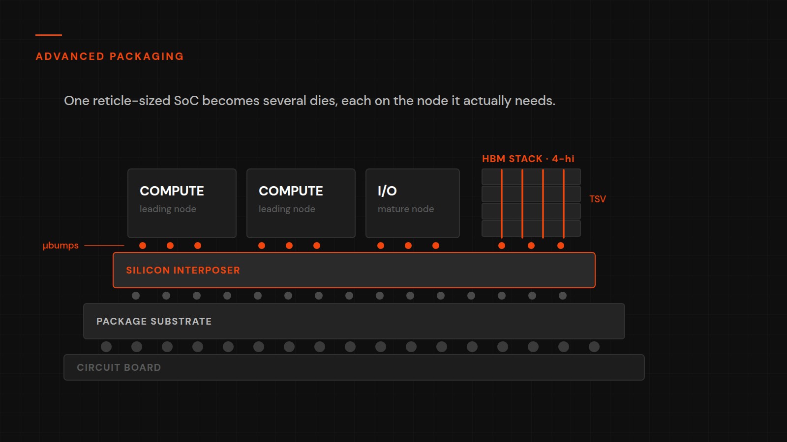
In a chiplet-based design, different functional blocks are implemented on different dies, each potentially manufactured on different process nodes optimized for that block's requirements. A typical high-end processor chiplet design might include: compute chiplets (CPU cores, GPU compute units, neural network accelerators) on the most advanced process node (TSMC N3 or N2) where transistor density and performance are most critical; I/O chiplets (PCIe controllers, DRAM interfaces, networking) on an older, cheaper process node (TSMC N6 or N7) where the analog-heavy circuits benefit from process stability rather than cutting-edge geometry; and memory chiplets (HBM stacks, SRAM caches) in a 3D stacked configuration directly on top of or immediately adjacent to the compute chiplets for maximum memory bandwidth.
AMD's EPYC Genoa (9004 series) processor is a clear example: the CPU compute cores are implemented in small "CCD" (Core Complex Die) chiplets manufactured on TSMC N5, while the I/O die (memory controllers, PCIe, infinity fabric hub) is manufactured on TSMC N6. This allows AMD to use the expensive advanced node only for the compute-intensive logic, reducing per-chip cost compared to a full-monolithic advanced-node design, while maintaining the performance of advanced-node compute.
Advanced Packaging Technologies — The Glue of Chiplet Architecture
The performance of a chiplet-based design depends critically on the interconnect bandwidth between chiplets. Inter-chiplet bandwidth must approach (or equal) on-chip interconnect bandwidth to avoid becoming a bottleneck. This requires advanced packaging technologies that go far beyond conventional wire bonding or even flip-chip BGA attachment.
2.5D Packaging (Interposer-based): Chiplets are mounted side-by-side on a silicon interposer — a thin silicon substrate with fine-pitch interconnect traces (2–10 µm pitch) that provides high-bandwidth connections between chiplets. TSMC's CoWoS (Chip-on-Wafer-on-Substrate) is the industry-leading 2.5D packaging technology, used in NVIDIA's H100/H200 GPUs (which integrate the GPU die with HBM memory stacks on a silicon interposer). CoWoS-S (silicon interposer) enables thousands of connections between chiplets at pitches that conventional PCB or even advanced substrate technology cannot achieve.
3D Stacking (Face-to-Face, Face-to-Back): Chiplets are stacked vertically with through-silicon via (TSV) connections providing vertical interconnect between layers. TSMC's SoIC (System on Integrated Chips) and Intel's Foveros enable 3D stacking of chiplets with TSV pitches in the single-digit micrometer range, providing far higher interconnect density than even 2.5D interposer approaches. AMD's 3D V-Cache (stacking additional SRAM cache directly on top of the CPU die using hybrid bonding) is a commercially deployed example that delivers substantial performance improvements for cache-sensitive workloads.
Hybrid Bonding: The most advanced interconnect technology, hybrid bonding uses direct copper-to-copper bonding between the top metal layers of two dies (without any solder bumps), enabling sub-micrometer bond pitch and therefore dramatically higher interconnect density than bump-based approaches. TSMC's SoIC-X and Intel's Foveros Direct both use hybrid bonding for their highest-bandwidth applications, enabling die-to-die interconnect bandwidths comparable to on-chip global wires.
The UCIe Standard — Making Chiplets Interoperable
One of the key challenges with chiplet-based design is die-to-die interface standardization. If every chiplet designer implements a proprietary die-to-die interface, chiplets from different vendors cannot be mixed in the same package without custom integration work. This defeats one of the key advantages of chiplet disaggregation — the ability to source chiplets from best-in-class suppliers and assemble them into a system package.
UCIe (Universal Chiplet Interconnect Express) is the industry standard being developed to address this. Published in 2022 and now on version 2.0, UCIe defines a standardized die-to-die interface covering physical layer specifications (bump pitch, signaling, power delivery), protocol layer (transport of PCIe or CXL traffic over die-to-die links), and software models. Intel, TSMC, AMD, ARM, Qualcomm, and Samsung are among the founding members of the UCIe consortium.
UCIe adoption is the key enabler for a genuine chiplet ecosystem — where SoC designers can select compute chiplets, I/O chiplets, and memory chiplets from different vendors and combine them into a custom package, similar to how PCB designers select components from different vendors today. This is an ongoing process as of 2026, but the industry is clearly moving in this direction.
Implications for Industrial and Embedded Electronics
Chiplet architecture and advanced packaging are initially appearing in high-end server, data center, and AI accelerator products — not in the embedded microcontrollers and SoCs that most industrial automation engineers work with daily. But the technology is diffusing toward embedded applications, and understanding the direction has practical value.
First, the edge AI chips that will power the next generation of industrial edge devices are being designed using chiplet principles. The ability to combine an advanced-node AI inference accelerator chiplet with a mature-node I/O chiplet and HBM memory in a compact package will enable edge AI chips with data center-class inference performance in industrial form factors. This is not speculation — companies like Hailo and Axelera are already exploring multi-die packaging for their next-generation products.
Second, heterogeneous integration — combining chips of different materials (silicon, GaN, SiC, InP) in a single package using advanced packaging techniques — is enabling new categories of mixed-signal and power electronics. Industrial power converters, motor drive systems, and RF modules are increasingly integrating silicon digital control with wide-bandgap power devices in single-package solutions using advanced packaging technology. This delivers better thermal performance, smaller form factor, and higher system efficiency than discrete component implementations.
When the system boundary moves inside the package
The habit worth breaking here is treating “the chip” as an atomic part. For a monolithic SoC that was a reasonable simplification. For a multi-die package it is no longer true, and a few practical consequences follow from taking it seriously.
The first is thermal. A package containing several dies with different power densities does not present a uniform heat source, and stacked configurations put heat-generating logic underneath other silicon. From the outside it is still “one component with a heatsink”, but the internal picture is uneven, and the thermal solution has to be designed against the component’s actual behaviour rather than a single averaged number. For sealed, fanless industrial enclosures, that distinction is not academic.
The second is that performance becomes less uniform in a way that matters for timing. In a disaggregated design, whether two pieces of work sit on the same die or communicate across a die-to-die link is a real difference in latency and bandwidth. For throughput-oriented workloads that averages out. For anything with a deterministic timing requirement, averages are the wrong statistic — what matters is the worst case, and the worst case now depends on topology inside the package.
The third is supply. A multi-vendor package has a correspondingly complicated supply chain, and “the part is available” becomes a question about several processes and an assembly capability rather than one. For industrial designs, where lifecycle and second-sourcing are first-class requirements rather than afterthoughts, that is a genuine consideration.
None of this is an argument against chiplets — the economics driving them are overwhelming, and the approach is plainly correct for high-performance silicon. It is an argument for reading the package-level documentation instead of the headline part number, and for the general principle that when a boundary moves, the assumptions built on its old position need re-examining. Designing from requirements and failure modes first is what makes that re-examination routine rather than a surprise.
Conclusion
Chiplet architecture and advanced packaging are now the default for high-performance semiconductor design, driven by the physical and economic limits of monolithic scaling and enabled by rapid progress in packaging. AMD’s multi-die EPYC processors, CoWoS-packaged accelerators, and effectively every new AI architecture make the point: this is production reality, not a research direction.
The shift worth carrying away is conceptual. A modern high-performance part is a system in a package, with internal structure that shows up as thermal behaviour, non-uniform latency and supply-chain complexity. Understanding that structure is becoming part of specifying a component properly — the integration work did not disappear when it moved inside the package.